FPGA Design Flow
An FPGA (Field Programmable Gate Arrays) is a programmable chip used in various industry applications such as 4G/5G Wireless systems, Signal Processing Systems, and Image Processing Systems. FPGAs are also used as accelerators for CPU, prototyping of ASIC designs and in Emulation.
The main advantage of using FPGAs is that they are highly customizable. FPGAs are available with ARM based CPU(s) along with associated high-performance interfaces like PCIe, 10/40G Ethernet, SATA, DDR3, QDR4 etc.
FPGA Architecture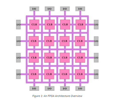
- FPGAs consist of three types of modules.
Configurable Logic Block (CLB)
It is a fundamental building block of an FPGA. Each CLB contains multiple slices. Each slice consists of function generators (LUTs), registers, multiplexers, carry logic etc. - Switch matrix or interconnection wires
Signals between CLBs and from CLBs to IOBs are routed through Switch matrices. - IO blocks (IOB)
An IOB is the basic input/output function block


Applications of FPGAs
FPGAs have a wide range of applications. Some of them are listed below
- Communications, Avionics, Missiles, Secure systems, high-end RADARs and Space applications.
- Portable electronics, Software Defined Radio, Digital Signal Processing, Speech recognition.
- High-resolution Video, Audio processing, Automotive infotainment.
- Switches & Routers, encoders & decoders, Servers, data center security.
- Digital camera, Set-top box, Multifunction printer, Digital display.
Typical FPGA Design Flow
1. FPGA Selection
Selection of an FPGA is the first step in the design phase. FPGA vendors have started to provide FPGA based on different end user applications like Automotive, Defence and Space Applications.
FPGA have also proven their utility in recent technologies like 5G Wireless, Embedded Vision, Industrial IoT and Cloud Computing, which are made possible due to the availability of ARM Processors and C based compilers for FPGA platforms.
| Category | Device |
|---|---|
| Xilinx Automotive (XA) | XA Zynq UltraScale+ XA Zynq®-7000 XA Artix®-7 Kintex® |
| Xilinx Defense-Grade | Artix®-7Q Kintex®-7Q Virtex®-7Q |
| Xilinx Space-Grade | Virtex-5QV Virtex-4QV |
2. Choosing an FPGA
FPGA resources are limited by the following parameters:
- Number of Available IO’s (Differential and Single Ended).
- Number of Internal memories (RAMs)
- DSP Slices (Complex Multipliers )
- Connectivity Ports (Serial Interfaces , Memory Interfaces)
Pin-compatible devices with higher resources need to be considered while choosing an FPGA for an evolving design, so that there is sufficient head-room in accommodating additional logic that may be necessary.
As a thumb rule, utilisation of 60% – 75% of logic resources like slices and LUTs could be considered as an upper limit – beyond this limit, designers tend to face issues related to routing congestion and timing closure.
3. Estimation
Estimating the resource utilisation helps in choosing a suitable FPGA as well as deciding about the BoM (Bill of Materials) for the overall system.
3.1- Area Estimation
Area Estimation is used to predict the occupancy of the FPGA device. Choosing a FPGA with a lesser gate count will be a major risk for the project since it puts the whole system (including the PCB that is developed based on the chosen FPGA) into trouble if we don’t fit the design into target FPGA.
Micoarchitecture of complete system targeted into FPGA will give us the number of modules and their internal sub-blocks. To provide the area estimate for a full design, we can start with the synthesis report of basic building blocks in design. Starting with smaller sub-blocks we can hand-code them and get the synthesis reports, which will give an approximate area of the block in the targeted FPGA (note that different families of FPGA have different architectures).
With the sub -blocks area estimation numbers in hand we can sum them up and get the area estimation for individual modules. Each FPGA device has inbuilt resources we should include their usage as well, during the estimation. Some of the in-built resources in FPGAs are:
- Memory [Block RAM’s].
- DSP Slices [Complex multipliers and Normal Multipliers]
- Number of IO’s at System Top level.
- Number of PLLs [Clocking block for System Clock].
- High Speed Interfaces GTX/GTH/GTP [Used for PCIe,Ethernet]
- Memory Interfaces [DDR Interfaces with Controller and PHY Interface]
3.2- Power Estimation
Board design and FPGA design are concurrent processes, so we need Power Budgeting numbers as early as possible. Some of the tools that assist in power estimation are:
- Xilinx Power Estimator (XPE) → pre-design & pre-implementation phases
- Vivado Power Analysis → post-synthesis, post-placement, and post-routing
- Xilinx Power Estimator assists with architecture evaluation, device selection, appropriate power supply components, and thermal management components specific for the targeted application.
Vivado Power Analysis helps to monitor power – as your design flow progresses through synthesis and implementation you will want to monitor and verify the power consumption regularly. We must ensure that thermal dissipation remains within budget so that we can detect and act early if any constraints are likely to be violated.
4. Design Entry
This phase involves design entry in certain formats which will be inputs to Design Synthesis stage. The various ways a design can be entered are
- RTL design in VHDL, Verilog, SystemVerilog, C-program etc.
- Schematic entry
- IP cores from third-party IP vendors or FPGA device vendors
- Simulation Libraries
5. Design Synthesis
Design synthesis will read the design entered, and will generate the Gate Level Netlist supported for implementation.
6. Design Implementation
Translate
During the translate stage of the implementation, all the netlists are merged into a single NGD (Native Generic Database) netlist file. It performs timing specification checks and logical design rule checks. It then adds constraints from the user constraint file (UCF) to the merged netlist.
Mapping
During this phase, the tool allocates CLB and IOB resources for all basic logic elements. The tool then processes location and timing constraints. It also performs target optimization and generates the physical design database or NCD (Native Circuit Description) file. It then provides a post-map STA report that describes all block delays and estimated routing delays.
Placement and Routing
Placement and Routing of the design is done in this phase. The output is the post-place-and-route STA report which lists all nets and delays in the design.
7. Device Programming
A configuration file is created depending on the target and settings specified. An FPGA device can be programmed directly from the host computer using a download cable or through flash/PROM.
Advanced FPGA Design Flow
An advanced FPGA flow is almost always desirable for high-speed or high-density designs.
In an advanced FPGA design flow, more sub steps of design flow are followed. More tools are used for better area and timing closure.
| Function | Eg Tools used |
|---|---|
| Logic equivalency check | Synopsys Formality |
| Floor planning and layout | Synopsys Amplify/ Xilinx FloorPlanner/ PlanAhead |
| Static Timing Analysis (STA) | Synopsys Primetime |
| Power calculation | Xilinx XPower |
| Editing the routing and placement | Xilinx FPGA Editor |
Conclusion
Running a design through a simple FPGA flow sometimes won’t be sufficient for complex designs. Therefore, for stringent design requirements like dense area or aggressive timing requirements or for other challenges like a large FPGA, we need to go through an advanced FPGA flow.
CoQube
In CoQube, we have the expertise and exposure to end-to-end development of complex FPGAs for diverse use models such as Intellectual Property (IP) development and embedded systems targeted to various domains including Communication (4G/5G). We can assist in multiple stages such as architecture definition, optimization, technology migration, interface bring-up, verification, system validation and hardware platform evaluation to name a few.
References
https://en.wikipedia.org/
https://www.xilinx.com/
Tree-based Heterogeneous FPGA Architectures by Farooq, Umer,Marrakchi, Zied,Mehrez, Habib