Clock Gating for Power Reduction
Low power design is a necessity today in all integrated circuits. Over time, semiconductor devices have packed more and more features (and transistors) in keeping with Moore’s law. For battery-operated devices (mobile/ handheld/ laptops), battery backup time has become an increasingly important criterion in influencing customers’ buying decisions.
As is well known, power dissipation has a direct relation to clock frequency. Dynamic power, which refers to the power consumed when a circuit is active, depends upon the rate at which signals toggle (switching activity). The more work the design does, the more energy it ends up needing. As the speed at which work is required to be completed increases, the dynamic power consumed increases too. To save dynamic power, we can either slow down the design (reduce clock speeds), try to reduce operating voltage, or attempt to cut down design activity.
Traditionally, designers left power minimization to implementation/physical tools, which come into play in the later parts of the design cycle. However, by then, all important architectural and micro-architectural decisions about the design have been frozen. Physical tools can influence power only in a limited way, unable to make sweeping changes to the design architecture.
By deploying power-saving techniques upfront in the design cycle, significant reduction in power consumption can be achieved. The rest of this document talks about one such technique for power reduction – Clock Gating.
Designer’s Role
The first task is to identify the High-Activity Nets – these are predominantly Clock signals in most digital designs. As mentioned earlier, dynamic power reduction is about choosing clock speeds and voltages and looking at activity. These factors can be addressed better at higher levels of design abstraction. Typically, design architects choose operating voltages and clock speeds. However, reducing clock activity (especially, unnecessary activity) is definitely an optimization parameter for the designer, and we will look at addressing that aspect. Many of these reductions require micro-architectural changes (such as FSM re-encoding, block-level clock gating, memory gating, memory banking, and bypassing memory accesses) that require a deep understanding of design functionality. These changes are better performed by the designers who develop the RTL.
In this document, we discuss Clock Gating as a technique for low power design, independent of EDA tools. We consider the design of a circuit that generates a control signal for clock gating. We discuss the evolution of the circuit through various intermediate stages to help clarify the underlying issues.
Handling the Clock Gating Control
Dynamic power can be reduced by reducing clock frequency, since it reduces signal transitions per unit time. However, this may not always be possible since this could adversely impact design performance (eg. data throughput). Alternatively, we can employ clock gating techniques, wherein a special enable signal is applied on the clock gating cells to turn ON or turn OFF the clock for a specific group of flops – this helps reduce dynamic power consumption.
Clock gating was one of the earliest techniques to used to save power. It results in area-savings where there is sharing of gating logic. However, it also makes the design slightly more complicated for timing analysis and DFT. The thought process here is that if a common clock signal is going to hundreds of flops and the functionality is such that a lot of them are just retaining their old values, then we can gate-off the clock to such groups of flip flops when possible and they still retain their old values. This gating-off results in lesser toggling in the clock path cells and thus saves dynamic power.
Handling the Clock Gating Cell
We now look at a scenario where architectural clock gating is required, with specific focus on generating the clock enable signal. When the design has only one clock source, and the clock enable signal is generated from a D-flip-flop, it is tricky to handle the assertion of the clock enable, since there won’t be any active clock to drive the enabling D-flip-flop.
1. Considerations
Figure1: Basic Interface of a Digital Design with a Clock Source
Consider the scenario in which an EXTERNAL clock source is providing a clock to the design and this source is controlled by an “ENABLE” (active high) signal.
When the design is not necessarily required to be functional, an asynchronous input signal to the design can be asserted to put it into a dormant mode. Let us call this signal “SHUTDOWN”. In turn, the design can request the external clock source to be turn the clock OFF. In effect, when the SHUTDOWN signal is asserted, the clock ENABLE should be de-asserted so as to turn OFF the clock. When SHUTDOWN is de-asserted the clock should be turned on.
A D-Flip-flop is used in the digital block for ENABLE generation. Typically, it has an active-low SET (SBAR) and active-low RESET (RBAR).
2. POWER-UP STATE
Let us consider an active-low power-on-reset (PORB, where the B stands for active-low, or ‘bar’) input to the design. On power-up the clock ENABLE is LOW (i.e. clock is gated off). Once PORB goes high, the ENABLE signal should be asserted to get the clock started.
Normally, asynchronous reset signals are synchronized using reset synchronizers before being used in the design. However, in this case, the asynchronous reset (PORB) has to be connected directly (without synchronisation logic) to the flip-flop generating the clock ENABLE signal, as the clock is not enabled at this point. Without a running clock, it is not possible to synchronize the reset with a reset synchronizer to get a synchronous reset.
ENABLE is an active-high signal. We need to get ENABLE asserted when the reset (PORB) is deasserted. Also, we need to get ENABLE cleared when the reset is asserted.
Consider a D flip-flop for ENABLE that has asynchronous active-low inputs for set (SBAR) and clear (RBAR). By connecting PORB to RBAR, we can get the ENABLE to be cleared on PORB assertion.
However, on PORB de-assertion, ENABLE remains LOW. To get ENABLE asserted after PORB deassertion, we need to assert SBAR. Again, since there is no active clock at this point, the event on SBAR should be created asynchronously. To accomplish this, we could use buffers, inverters and a few basic logic gates as shown in the figure below.
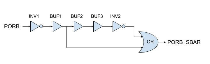
Figure2: Asynchronous PORB de-assertion event creation circuit for driving SBAR

Figure3: Clock ENABLE Handling Cell – Stage 1

Figure 4: Timing Diagram of ENABLE behaviour on Assertion and De-assertion of PORB
NOTE : Since the above logic has buffers, there are high chances of a synthesis tool optimizing the design and removing all the buffers since that wont alter the logic function.
As these buffers are library cells, set_dont_touch should be added on these cells as part of synthesis constraints so as to prevent their removal by the tool. This is very important since the number of buffers put in the logic are decided so as to meet the set/reset port timing of the flip-flop. Note that the number of buffers has a direct impact on the width of the LOW pulse on PORB_SBAR. Too few buffers may result in the D-flip-flop not detecting the pulse.
3. Disabling clock on SHUTDOWN event
As mentioned earlier, an external event can request the device to get into SHUTDOWN mode at any time. When the device is in SHUTDOWN mode, since the device is not functional, the clock can be turned OFF, thereby reducing dynamic power.
Typically, the SHUTDOWN request is received when the device is operating, which means the design has a clock input that is active (turned-on). Hence it is a good and safe design practice to synchronise the SHUTDOWN input and use the synchronised version to de-assert the ENABLE signal as shown in Figure 5 below (as against connecting it to RBAR pin through combinational logic that also uses PORB). Here SHUTDOWN_SYNC is the double-synchronised version of the SHUTDOWN signal.

Figure5: Clock ENABLE Handling Cell – Stage 2
4. Handling FSMs before disabling clock
Almost every digital design has multiple state machines for functional operation. If the clock is gated-off immediately after the SHUTDOWN event, the FSMs may get stuck in their current states. When the SHUTDOWN event is removed and the clock is restarted, there could be a functional failure, since the FSMs would start from non-IDLE states.
This should be taken care as a part of FSM design. The FSMs should be designed in such a way that on detecting a SHUTDOWN event, they gracefully complete any on-going transactions and give out status flags (eg. FSMx_DONE) to indicate that the FSMs are now in IDLE state.
These flags, along with the SHUTDOWN_SYNC signal can be used to turn OFF the clock as shown in Figure 6 below, ensuring that all the state machines wake up in their IDLE states when the SHUTDOWN event is removed.

Figure 6: Clock enable handling cell – Stage 3
5. Enabling clock on exit from shutdown
Enabling the clock on de-assertion of SHUTDOWN can be handled in a similar way to PORB de-assertion mentioned earlier. Since SHUTDOWN is an active-high signal, the event can be created with a little modification to the circuit shown in Figure 2. The modified circuitry is shown in Figure 7 and the waveforms for this circuitry are shown in Figure 8.

Figure 7: Circuitry to create an asynchronous SHUTDOWN de-assertion event for enabling clock

Figure 8: Waveforms for SHUTDOWN de-assertion event circuitry

Figure 9: Clock-enable handling cell – Stage 4
6. Inclusion in DFT scan chain
Since this cell is a very important part of the whole design that handles the clock, the inclusion of this cell in the scan chain is equally important so as to detect the manufacturing defects or faults.
In general, the basic signals required to support scan-based testing are DATAIN (SCAN_IN), DATA_OUT (SCAN_OUT), RESET (SCAN_RESETN – assuming an active-low scan reset), ENABLE (SCAN_ENABLE), SCAN_MODE and CLOCK (SCAN_CLOCK).
The challenge here is for all these scan-related signals to be multiplexed to the respective ports of the D-flip-flop in the clock-gating circuitry as a part of scan-chain build. The D-flip-flop has both SET (SBAR) and RESET (RBAR) ports, but there is only a RESET (SCAN_RESETN) available in SCAN mode. Hence, the logic on the SBAR input of the flop will need to remain unchanged. This is a problem as the SBAR pin is an asynchronous input and any activity on this port when scan testing is in progress will break the scan testing process by introducing unexpected changes at the flop output.
This challenge can be addressed by keeping the SBAR port disabled in scan mode. That is, as SBAR is an active-low pin, it should be driven to 1 in scan mode so that it does not cause any change in the flop’s behaviour during scan mode.

Figure 10: Clock enable handling circuitry – with scan insertion logic
Conclusion
If you don’t need a clock running, shut it down.
Clock Gating is one of the many energy-saving techniques which designers can use. But there is no silver bullet in low-power design. There are a lot of techniques and different methods one can use to attack different portions of the power equation. They usually have overhead of some sort. Some may have no overhead, some may affect the design area, and some may affect the operating speed. Users will have to mix and match many techniques to come up with a low-power methodology that works for them. The clock gating circuitry illustrated in this document is one example of a technique that helps in reducing dynamic power consumption.